Stocks● Neutral
dorsaVi Starts Silicon Run on RRAM Validation Chip, Targets 22nm Next
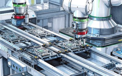
dorsaVi (ASX:DVL) starts fabrication of its first RRAM-CMOS validation chip, a 180nm run that de-risks the 22nm program with NTU and ITRI for physical AI applications.
Continue with
dorsaVi (ASX: DVL) has begun physical manufacturing of its first resistive random-access memory (RRAM) validation chip, moving the program from design into an active silicon wafer run. The company confirmed that its manufacturing data package passed foundry intake and the wafer lot is now in fabrication on the front-end CMOS base.
The current run uses a 180nm node. That base layer will support the RRAM memory array, peripheral circuits, and evaluation features before the RRAM-specific layers are added in a later stage. dorsaVi is taking a staged approach, generating process knowledge at each step before moving to the next. The goal is to produce silicon-level electrical testing results and performance benchmarks that can de-risk a subsequent 22nm program developed with NTU and ITRI.
Foundry acceptance means the design files, mask data, process documentation, and wafer-lot instructions all met the intake requirements. The CMOS base now being produced will provide the foundation for back-end-of-line preparation, RRAM stack integration, and formation of the integrated memory cells and arrays. Once the base is complete, the wafers are expected to move into partner-led processing and integration before electrical testing and characterisation assess how the completed architecture performs.