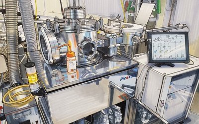
Adisyn has achieved a milestone in material science by demonstrating the continuous formation of graphene films at temperatures below 450°C. Utilizing Atomic Layer Deposition (ALD), the company successfully produced a 1cm x 1cm graphene film. This development addresses a critical thermal threshold in semiconductor manufacturing, where high-temperature processes have historically limited the integration of carbon-based materials into standard silicon-based production lines.
Thermal Constraints and Material Integration
The semiconductor industry relies heavily on copper for interconnects, which serve as the conductive pathways between transistors. As device scaling continues to shrink, copper faces physical limitations, including increased resistance and electromigration issues. Graphene offers superior electrical conductivity and thermal stability, but its synthesis typically requires temperatures exceeding 800°C. These high temperatures are incompatible with the back-end-of-line processing steps in modern chip fabrication, which must remain below 450°C to prevent damage to existing transistor structures.
By lowering the synthesis temperature, Adisyn’s approach aligns with the thermal budgets of current foundry processes. This compatibility is essential for the adoption of graphene as a replacement or supplement for copper in high-performance computing and advanced logic chips. The ability to deposit continuous films at these temperatures could allow manufacturers to integrate graphene without requiring a complete overhaul of existing fabrication infrastructure.
Scaling and Manufacturing Viability
While the 1cm x 1cm film represents a proof of concept, the transition to wafer-scale production remains the primary hurdle for commercial viability. The use of ALD is a strategic choice, as this technique is already standard in semiconductor manufacturing for depositing thin, uniform layers of material. The process offers precise control over film thickness and uniformity, which are prerequisites for reliable interconnect performance.
Key technical milestones for the next phase of development include:
- Achieving consistent film uniformity across 300mm wafers.
- Demonstrating adhesion properties compatible with standard dielectric materials.
- Reducing defect density to meet industry standards for signal integrity.
AlphaScala data currently tracks various technology sector participants, including ASE Technology Holding Co., Ltd., which holds a Moderate Alpha Score of 70/100. As the industry monitors advancements in commodities analysis and material science, the focus will shift toward whether Adisyn can move from laboratory-scale samples to pilot-line integration. The next concrete marker for this technology will be the publication of data regarding the electrical resistivity of these low-temperature films compared to standard copper interconnects, as well as any partnerships formed with semiconductor foundries to test the material in a production environment.